Understanding how 2022 CPU works as noob
CPU design is pretty complex in modern world (M1, Intel big little, AMD chiplet) and looks nothing like what I learned in computing architecture back when I was young. In the past few months I read some good articles and wanted to write some of my understanding down.
Also note that I am not a CPU architect designer, nor do I work in related industry. I am just a random dude who happens to assemble a dozen of workstations, servers and spent a lot of time watching Youtube CPU reviews.
A basic understanding of simple CPU
So what a CPU does is do calculation : addition and moving data around. So in order to tell the CPU what to do, you need a set of rules and format to follow so everyone can follow. The rest are just abstraction or syntax sugar for the gen Z.
I try to be simple and skip something here because I need to spent the space on discussing “modern” CPU design

Instruction
Suppose you have some input store somewhere with the address of that data and you want to do an operation on these data ( addition, subtraction, division, move to other address ). You need to write these command.
So this is where instruction come to play.
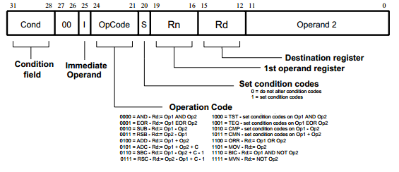
As of the 2022 modern world, we had x86 (CISC), ARM (RISC) making up the majority of CPU we use. Although the differences are becoming more blurred
Arithmetic logic unit (ALU)
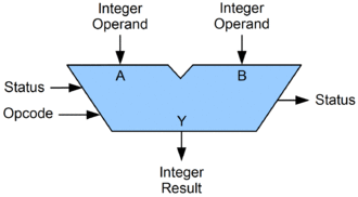
Once you know the instruction, a CPU can now parse these instruction and pass it to an ALU to do calculation. An ALU basically takes care of the addition, subtraction… all the math operations.
Execution Pipeline
So you have a instruction you wish to run, what steps are you going to do?
The steps of a CPU instruction can be broken down into the following phases:
-
Fetch: The CPU retrieves the next instruction to be executed from memory.
-
Decode: The CPU decodes the instruction to determine what operation it specifies.
-
Execute: The CPU carries out the operation specified by the instruction.
-
Store: The CPU stores the result of the operation in memory or in a register.
These steps are typically performed in a repeating cycle known as the fetch-decode-execute cycle, which allows the CPU to continuously execute instructions and perform operations on data. The speed at which the CPU can perform this cycle is known as the clock speed, and is measured in hertz (Hz). The faster the clock speed, the more instructions the CPU can execute per second.
However we doesn’t want to do only math function, we also want to do series of functions sometimes repeatedly. So we had Accumulator, that is used to hold the result of arithmetic and logic operations performed by the CPU. In most cases, the accumulator is a register that is used to store the result of an operation performed on data from memory or from another register. The accumulator is an important part of the CPU because it allows the CPU to perform a wide range of operations on data without having to constantly read and write to memory, which would slow down the computer’s performance.
Microcode engine (decoder)
As CPU design became more complex, the control logic for executing an instruction started becoming more complex and bigger. Hence microcode design was proposed to act as a abstraction between instruction and machine pipeline execution. Microcode optimization has since be one of the key optimization in many Intel CPU releases since 8086 (1978).
In modern CPU, the microcode is what drives the decoder section inside the CPU.
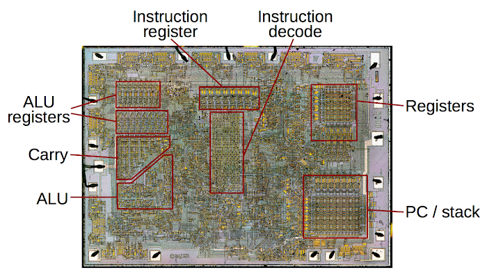
And here’s a i7-6700K die shot:
In modern CPU, the microcode is what drives the decoder section inside the CPU. | And here’s a i7-6700K die shot:
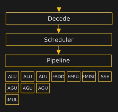
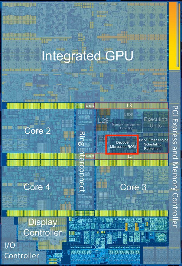
On the left, the microcode is what drives the decoder section inside the CPU (source). While on the right is a i7-6700K die shot, the microcode decoder is highlighted in red rectangle. Each core has their own microcode decoder.
I decided to skip multiplexor, scheduler, accumulator, register, how does an instruction work…, just google yourself. You are here for the “modern” part.
Modern tricks that make your CPU fast
As you might have noticed, a more modern CPU doesn’t look like this (source) 8008 CPU by Intel in 1983.
But this (source)
Much have changed since and I will elaborate some of the major changes that shape our modern CPUs.
Do note what I am showing here is only the tip of an iceberg and are only those which are interesting. If you wish to go down the rabbit hole here’s some keyword that can kept you busy : NUMA topology, big LITTLE, Re-order buffer.
Multi thread
Multithreading is a technique used by computer systems to improve the performance of certain types of applications. It involves allowing a single CPU, or central processing unit, to execute multiple threads of execution concurrently. Each thread represents a separate sequence of instructions that can be executed independently of the other threads. By executing multiple threads concurrently, the CPU can improve its overall performance and make more efficient use of its resources. This is because it can switch between threads whenever one thread is waiting for input or output, allowing it to continue executing useful work even when some threads are idle.
SMT
SMT, or simultaneous multithreading, is a variant of multithreading that allows each physical CPU core to execute multiple threads simultaneously, rather than just one thread per core as in traditional multithreading. This allows the CPU to make more efficient use of its resources and improve its overall performance by allowing more work to be done in parallel. SMT is often used in applications that need to perform multiple tasks concurrently, such as web servers and media players.
Both multithreading and SMT are important techniques for improving the performance of modern computer systems, and they are used in a wide range of applications. These techniques allow CPUs to execute more instructions in parallel, which can improve the overall speed and efficiency of the system.
IBM Power CPU has 4 SMT (or 8) as compare to the typical 2 SMT (1 core running 2 threads at the same time). As discuss in this reddit thread.
Branch predictor
Branch instructions are a type of instruction that can cause the CPU to branch to a different part of the program and execute a different sequence of instructions depending on the result of a conditional test. For example, a branch instruction might be used to check if a number is greater than zero, and if it is, the CPU will branch to a different part of the program to execute a different set of instructions. Branch predictors are used to improve the performance of the CPU by predicting the outcome of branch instructions and speculatively executing the appropriate instructions before the result of the branch is known for sure.
TLDR; Predict the outcome of the branch (where do your instruction jump to next, for example : if-else logic ) in order to execute the branched instruction section while you wait for the predict branch to finish. If your predictions are incorrect, you need to fallback and execute the correct instruction.
This allows the CPU to avoid stalling and continue executing useful work while it waits for the result of the branch instruction.
The longer your branch pattern and branch count are, the worse branch predictor performs. You can see it quite clear in this i5-6600k branch predictor visualization by clamchowder

Speculative execution
Following the jazz of branch predictor, we can also predict what instruction you will need to execute next and run it first. If the prediction turns out to be correct, the results of the speculative execution can be used immediately, which can improve the overall performance of the CPU. If the prediction is incorrect, the results of the speculative execution are discarded and the correct instructions are executed instead. Speculative execution is a complex and highly optimized process that is essential to the performance of modern CPUs.
If you ever heard of Meltdown/Spectre, this is the part where designers fucked up which lets hackers to access unauthorized section of memory address. Intel releases a microcode patch which claims to have fix this issue with a 6-10% worse performance (source). We can safely assumes that speculative execution contributes at least the same margin of speedup.
Tiered cache (L0-L3,4 cache)
One unsung hero of double digit improvements over generations in CPU/GPU since 2019 must be the cache size increase.
Once CPU/GPU started became very efficient at number crunching, they will soon bottleneck by how fast the data can be fetched to keep them fully ultized. This is where tiered cache such as L0, L1, L2, L3 cache come into play. By storing some frequently accessed data and instructions near the ALUs, the idle time can be reduced significantly. However you also risk spending precious time searching each different cache level while you can fetch it from the memory.
| Previous generation | New generation | Improvements* | |
|---|---|---|---|
| Nvidia 90 series | L2 6MB (3090) | L2 72MB (4090) | 42% |
| Intel i9 | 30MB (12900k) | 37MB (13900k) | 13% |
| AMD ryzen 8 | 32MB (5800X) | 96MB (5800X3D) | 15% |
| Apple M1 series | 16MB (M1) | 48MB (M1 Max) | 0-1% |
Note : Improvements varies by benchmark and cannot be compared across different compute from different designs; single core benchmarks are taken for CPU.
For a very long time, cache was seen as a good to have but not important element (Intel cache size was stagnant for quite a while). I think there’s two major element at play here : low core count and cache space.
Since AMD releases their Zen CPU, cache size has been increasing generation over generation due to more core needing to cache more data. However cache also populate precious space on the CPU die which the cost increases exponentialy by area (the larger your die is the higher the cost). IBM was able to work around this by offering their own internal SRAM design (yes all the L0-L3 cache are assembled from many SRAM cells), for a long time are the smallest cell in the industry. I think is at the expense of more complex manufacturing process hence higher cost.
IBM show casing 256MB of L3 cache on HotChips 33
It was until recently TSMC was able to offer their SRAM design which is dense enough for IC designers to own the luxury of large cache size. As well as the new 3D Fabric which allows SRAM to be stacked on top of the CPU die.
More materials
Writing about the interiors of modern CPUs has been on my TODO list for a while. While I tried my best to elaborate on these concepts, ultimately executing the final results on the final product (CPU/GPU) are done by thousands of engineers and collaboration across different fields ( signal integrity, semiconductor fab … )
Here are a dozen of sources I usually read to keep up with the latest advancement in modern computing:
-
Moore’s Law Is Dead - Youtube channel
Good for rumours, consistently accurate enough to plan out my future builds.
-
They have pretty detail benchmarks for new product release.
Footnote:
This article is cowritten by ChatGPT in small sections to speed up my narrative writings. ChatGPT does not guide any of my writing direction and opinions.